Basic directions
- Creating standards for relief solid surface.
- Study of influence of micro-and nanorelief of surface on the physical processes and phenomena occurring on the solid surface.
- Development of methods for measuring the linear dimensions of landscape elements in the scanning electron (SEM) and atomic force microscopes (AFM).
- Development of methods for calibrating SEM and AFM.
Application of research
- Micro-and nanotechnology.
- Metrology of linear measurements of the dimensions of landscape elements in the nano range.
- Calibration of scanning electron and atomic force microscopes.
- Scanning systems and positioning of micro-and nano range.
Creating standards of the relief surface for solid objects
To address the challenges, that laboratory is facing , embossed surfaces with a certain shape and size of the relief were created :
- Single grooves in silicon with parallel walls.
- Stepping structures on the silicon surface as a set of trapezoidal protrusions and grooves.
- Single grooves in silicon with parallel walls.
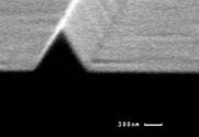
The distance between the walls can be from 50 to 500 nm, and the depth - 100 nm - 20 microns. Deviation from parallelism throughout the depth of less than 1 nm. The error in measuring the width of the groove is 0,3 - 1,0 nm. The figure shows an image in a scanning electron microscope cleaved single-groove width of 150.7 nm and a depth of 850 nm.
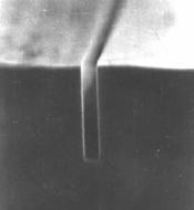
The image in a scanning electron microscope cleaved single-groove width of 150.7 nm and a depth of 850 nm
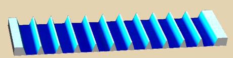
Stepping structures on the silicon surface as a set of trapezoidal protrusions and grooves are a series of grooves in monosilicon, the side walls of which are the crystallographic (111) planes of silicon, the top protrusion and bottom of the grooves between them - the crystallographic planes (100) silicon (see diagram in Figure ). Step size is 2000 nm. The dimensions of the upper bases of projections may be in the range 10 - 500 nm. The errors of appraisal dimensions of the elements of step structures (step structure, the size of the upper and lower bases of protrusions and grooves and the depth of the relief) is 1 nm.
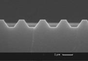
The figure shows an AFM image of a periodic structure on the surface monosilicon consisting of trapezoidal protrusions, the size of the upper base of which are 30 nm

The developed technology for producing such structures can make them with different sizes of the upper base of the projections in the range 10 - 500 nm and heights of the relief in the range 100 - 1500 nm.
(а) (б) (в)
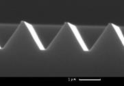
The figure shows the SEM image of incision of periodic structures elements with different heights and widths of the protrusions.
  
(а) (б) (в)
Figure shows AFM images of individual elements of the periodic structures with different width and height of the ledges. The dimensions of the upper bases projections in Figure 4 and 5 are 520, 110 and 30 nm respectively for figures (а), (б) and (в).
Such structures are the standard of relief in nano range, because boundary structures are set in natural settings (the crystallographic planes and angles between them). The quality of the structures that were so high that these structures are recognized as state standards (ГОСТ Р 8.628-2007 и ГОСТ Р 8.629-2007).
The influence of micro-and nanorelief surface on the physical processes and phenomena occurring at the solid surface
Study of influence of surface topography on the physical processes that led to the discovery of a new mechanism of secondary electron emission, called the "effect of shaking off" of surface electrons. This mechanism has a unique feature - the emission of secondary electrons from surface states occurs only when there is a transition of primary electrons from the vacuum to the solid. When the transition of the primary electrons is from a solid to a vacuum, emission of secondary electrons from surface states does not occur. The contribution of this mechanism in the full effect of the emission of secondary electrons can reach 30 - 70% (for silicon). The influence of the effect of shaking off is particularly strong for relief surfaces. In this case, the contribution of the effect of shaking off may reach 100%.
Using these studies have been established model of image formation of relief surfaces in the scanning electron microscope, which allowed us to develop methods of calibrating the SEM with rectangular and trapezoidal relief structures and methods of measurement of linear dimensions on the nanometer SEM. Originality and quality established calibration methods SEM led to the creation on their basis of national standard (ГОСТ З 8.631-2007).
Studies of interaction of the probe of an atomic force microscope with a relief surface and image formation in the AFM allowed the development of methods AFM calibration in all three coordinates and measurements on them, the linear dimensions of the relief elements in the nano range. The originality and quality of established methods for calibrating the AFM led to the creation on their basis of national standard (ГОСТ Р 8.630-2007).
For the creation of relief surfaces of nano range with controlled relief, study their properties, development of methods for calibrating the SEM and AFM and the development of methods for measuring linear dimensions in the nano range, the Head of the Laboratory A.V. Rakov, and chief researcher A. Novikov have been awarded with the Prize the Government of the Russian Federation in 2003 in science and technology.
The most important achievements of the laboratory
- Creation of standarts for relief surface of solids, based on their natural parameters.
- Discovery and investigation of a new mechanism of secondary electron emission - shaking off effect for surface electrons.
- Development of a model of forming a relief image of solid surface in a scanning electron microscope, taking into account the effect of shaking off.
- Development of methods for calibration of scanning electron microscopes (mesuring of magnification and size of an electron probe in two coordinates) to operate in the nano range.
- Development of methods for measuring the linear dimensions in nano scale for scanning electron microscope.
- Development of methods for calibration of atomic force microscope (dinining of a scale unit in all three coordinates, linearity and orthogonality of the scanning radius of cantilever tip) for operations in the nano range.
- All created structures and practices brought to the implementation, including up to the adoption of state standards.
Publications
2012-2013
- Кальнов В.А., Новиков Ю.А., Орликовский А.А. Работа электронного литографа в режиме растрового электронного микроскопа. // Микроэлектроника. 2012. Т. 41. № 6. C. 426-429.
- Новиков Ю.А. Виртуальный растровый электронный микроскоп. 1. Цели и задачи виртуальных приборов. // Микроэлектроника. 2013. Т. 42. № 1. C. 34-41.
- Новиков Ю.А. Виртуальный растровый электронный микроскоп. 2. Принципы построения прибора. // Микроэлектроника. 2013. Т. 42. № 4. C. 262-270.
- Новиков Ю.А. Разрешение растрового электронного микроскопа: 1. Современное состояние проблемы. // Поверхность. Рентгеновские, синхротронные и нейтронные исследования. 2013. № 5. С. 105-112.
- Новиков Ю.А. Разрешение растрового электронного микроскопа: 2. Измерение разрешения с помощью структур с прямоугольным профилем рельефа. // Поверхность. Рентгеновские, синхротронные и нейтронные исследования. 2013. № 8. С. 105-112.
- Новиков Ю.А. Измерение нелинейности сканирования в растровом электронном микроскопе. // Поверхность. Рентгеновские, синхротронные и нейтронные исследования. 2013. № 11. С. 70-74.
2011
- Новиков Ю.А. Изображение тест-объекта с трапециевидным профилем и большими углами наклона боковых стенок в РЭМ в обратно рассеянных электронах. // Поверхность. Рентгеновские, синхротронные и нейтронные исследования, 2011, № 10, с. 5-11.
2009-2010
- Filippov M.N., Novikov Yu.A., Rakov A.V., Todua P.A. SEM Probe Defocusing Method of Measurement of Linear Sizes of Nanorelief Elements. // International Conference “Micro- and nanoelectronics 2009”, Russia, Proceedings of SPIE, 2010, v. 7521, p. 752116-1 – 752116-9.
- Gavrilenko V.P., Novikov Yu.A., Rakov A.V., Todua P.A. Test objects for calibration of SEMs and AFMs operating at the nanoscale. // International Conference “SPIE Photonics Europe 2010”, Belgium, Proceedings of SPIE, 2010, v. 7718, p. 77180Y-1 – 77180Y-12.
- Gavrilenko V.P., Novikov Yu.A., Rakov A.V., Todua P.A. Accuracy of ellipsometric measurements of Si-SiO2 structures. // International Conference “SPIE Photonics Europe 2010”
- Ларионов Ю.В., Соколов В.О., Плотниченко В.Г. О механизме индуцированного изменения показателя преломления в фосфоро-силикатном стекле. // Квантовая электроника. 2010. Т. 40. № 3. С. 264-268
- Ларионов Ю.В. Роль точечных дефектов в фоточувствительности фосфоро-силикатного стекла, насыщенного водородом. // Квантовая электроника. 2010. Т. 40. № 5. С. 441-448.
- Валиев К.А., Гавриленко В.П., Жихарев Е.Н., Данилова М.А., Кальнов В.А., Ларионов Ю.В., Митюхляев В.Б., Орликовский А.А., Раков А.В., Тодуа П.А., Филиппов М.Н. Измерение линейных размеров кремниевых элементов нанорельефа с профилем, близким к прямоугольному, методом дефокусировки электронного зонда РЭМ. // Микроэлектроника. 2010. Т. 39. № 6. С. 1–7.
2008
Issues
- Новиков Ю.А., Раков А.В., Тодуа П.А. Прямое измерение ширины линии на атомно-силовом микроскопе. // Измерительная техника, 2008, № 5, с. 10-12.
- Новиков Ю.А., Раков А.В., Тодуа П.А. Калибровка АСМ по трем координатам с использованием одного аттестованного размера. // Измерительная техника, 2008, № 5, с. 13-15.
- Новиков Ю.А., Раков А.В., Тодуа П.А. Измерение линейности сканирования в атомно-силовом микроскопе. // Измерительная техника, 2008, № 6, с. 12-14.
- Новиков Ю.А., Раков А.В., Тодуа П.А. Точность измерения линейных размеров на растровых электронных микроскопах в микро- и нанотехнологиях. // Измерительная техника, 2008, № 6, с. 15-18.
- Волк Ч.П., Новиков Ю.А., Раков А.В., Тодуа П.А. Калибровка растрового электронного микроскопа по двум координатам с использованием одного аттестованного размера. // Измерительная техника, 2008, № 6, с. 18-20.
- Данилова М.А., Митюхляев В.Б., Новиков Ю.А., Озерин Ю.В., Раков А.В., Тодуа П.А. Тест-объект с шириной линии менее 10 нм для растровой электронной микроскопии. // Измерительная техника, 2008, № 8, с. 20-23.
- Гавриленко В.П., Новиков Ю.А., Раков А.В., Тодуа П.А. Тест-объекты с прямоугольным и трапециевидным профилями рельефа для растровой электронной и атомно-силовой микроскопии. // Наноиндустрия, 2008, № 4, с. 24-30.
- Новиков Ю.А., Раков А.В., Тодуа П.А. Геометрия формирования изображения в сканирующей зондовой микроскопии. // Микроэлектроника, 2008, т. 37, № 6, с. 448-469.
- Гавриленко В.П., Новиков Ю.А., Раков А.В., Тодуа П.А. Метрология и стандартизация в нанотехнологиях. // Заводская лаборатория, Диагностика материалов. 2008, т. 74, Спец. выпуск, с. 31-41.
Presentations at international conferences
- Раков А . В ., Новиков Ю . А . International Conference “Instrumentation, Metrology, and Standards for Nanomanufacturing”, San Diego, USA, 2008.( 3 устных доклада) .
- Раков А.В., Новиков Ю.А. NanoScale 2008. 8th Seminar on Quantitative Microscopy and 4th Seminar on Nanoscale Calibration Standards and Methods. Torino, Italy, 2008. (2 стендовых доклада ).
- Gavrilenko V.P., Mityukhlyaev V.B., Novikov Yu.A., Ozerin Yu.V., Rakov A.V., Todua P.A. Test object of the linewidth with a trapezoidal profile and three certified sizes for a SEM and AFM. // NanoScale 2008. 8th Seminar on Quantitative Microscopy and 4th Seminar on Nanoscale Calibration Standards and Methods. Programme and Short Abstracts. Torino, Italy, 2008. p. 51.
- Gavrilenko V.P., Novikov Yu.A., Rakov A.V., Todua P.A. Test objects with right-angled and trapezoidal profiles of the relief elements for SEM and AFM. // NanoScale 2008. 8th Seminar on Quantitative Microscopy and 4th Seminar on Nanoscale Calibration Standards and Methods. Programme and Short Abstracts. Torino, Italy, 2008. p. 59.
Presentations at russian conferences
- Новиков Ю.А., Раков А.В., Тодуа П.А. 22 Российская конференция по электронной микроскопии, Черноголовка, 2008. (1 устный и 8 стендовых докладов
- Гавриленко В.П., Лесновский Е.Н., Новиков Ю.А., Раков А.В., Тодуа П.А., Филиппов М.Н. Первые российские стандарты в нанотехнологии. // 22 Российская конференция по электронной микроскопии, Черноголовка, ИПТМ РАН, 2008, Тезисы докладов, с. 22.
Митюхляев В.Б., Новиков Ю.А., Озерин Ю.В., Раков А.В., Тодуа П.А. Тест объект ширины линии для РЭМ и АСМ с тремя аттестованными размерами. // 22 Российская конференция по электронной микроскопии, Черноголовка, ИПТМ РАН, 2008, Тезисы докладов, с. 101.
Новиков Ю.А., Раков А.В., Тодуа П.А. Калибровка АСМ по трем координатам с помощью одного аттестованного размера. // 22 Российская конференция по электронной микроскопии, Черноголовка, ИПТМ РАН, 2008, Тезисы докладов, с. 102.
- Новиков Ю.А., Раков А.В., Тодуа П.А. Определение линейности сканирования в атомно-силовом микроскопе. // 22 Российская конференция по электронной микроскопии, Черноголовка, ИПТМ РАН, 2008, Тезисы докладов, с. 103.
- Новиков Ю.А., Раков А.В., Тодуа П.А. Прямое измерение ширины линии на атомно-силовом микроскопе. // 22 Российская конференция по электронной микроскопии, Черноголовка, ИПТМ РАН, 2008, Тезисы докладов, с. 104.
- Новиков Ю.А., Раков А.В., Тодуа П.А. Контроль качества изготовления тест объектов с трапециевидным профилем на РЭМ. // 22 Российская конференция по электронной микроскопии, Черноголовка, ИПТМ РАН, 2008, Тезисы докладов, с. 105.
- Новиков Ю.А., Раков А.В., Тодуа П.А. Тест объекты с прямоугольным и трапециевидным профилями элементов рельефа для РЭМ и АСМ. // 22 Российская конференция по электронной микроскопии, Черноголовка, ИПТМ РАН, 2008, Тезисы докладов, с. 106.
- Митюхляев В.Б., Новиков Ю.А., Раков А.В., Тодуа П.А. Изображение меры МШПС-2.0К в обратно рассеянных электронах. // 22 Российская конференция по электронной микроскопии, Черноголовка, ИПТМ РАН, 2008, Тезисы докладов, с. 139.
- Митюхляев В.Б., Новиков Ю.А., Озерин Ю.В., Раков А.В., Тодуа П.А. Кремниевые тест объекты с размерами рельефных элементов менее 10 нм. // 22 Российская конференция по электронной микроскопии, Черноголовка, ИПТМ РАН, 2008, Тезисы докладов, с. 140.
|

