|

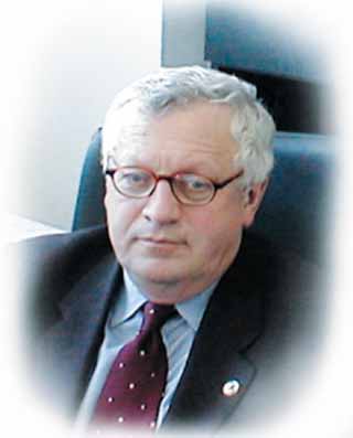
Director of Natural Sciences Center of General Physics Institute, Professor, Full member of RAS [Russian Academy of Science]
Vitaly Ivanovich Konov |
.....Natural Scienses Center (NSC) was established in 1996 at the initiative of Academician A.M. Prokhorov as a scientific institution engaged in basic research at the intersection of physics and other sciences - chemistry, biology, medicine and environment. As a top priority of the Center from the very beginning nanophysics and nanotechnology were announced. Now the basic scientific directions of the Center are:
- Atomic scale, Measurement and Technology, nanolithography
- Synthesis, properties and applications of diamond, carbon nanotubes and other new carbon materials
- Interaction of radiation with matter, spectroscopy
- Optical diagnostics of biological tissues and photodynamic therapy
- Sensors
- Electrophysics
Essential element of the Center activity is work in the field of advancement of results of researches on the market of high technologies. The original concept is realized in the Center. It is based on the symbiosis of a scientific establishment and small venture companies under one roof, which leads the numerous developments of the Center to the market product and successfully they compete on the national and foreign markets.
In the lifetime of the Center colleagues published more than 600 scientific articles, prepared and defended 8 doctoral and 21 candidate dissertations, more than 40 patents are obtained.
Employees are awarded by high scientific awards, including: the State Award of the Russian Federation (Konov V.I.), the Award of the Government of the Russian Federation (Rakov A.V., Novikov Y.A.), the State Award of the Russian Federation for Young Scientists (Kononenko V.V.) and others.
The Center structure includes following departments:
Laser Physics
Light-induced surface phenomena
Department of Technology and the measurement in atomic scale
Total number of employees of the Center - 108, the number of scientific workers - 76,
Members RAN [Russian Academy of Science] - 1, the number of doctors of sciences - 11, Candidates of Sciences 50,
graduate students and competitors - 18, students – 34.
1. UHV probe microscopy of atomic resolution, development for methods of atomic construction of crystalline materials. .
- The mechanisms of surface chemical reactions at the atomic level are studied based on the example of interaction of I2 and Cl2 with single crystals Ag, Cu, Si, GaAs. A number of technological methods, which make it possible to govern the atomic structure of surface is developed and locally, with the atomic accuracy, to move away the material, for example, silicon.
- The method of the gigantic (up to 1000 times) enhancement of the signal of Raman scattering in the tunneling gap was developed and realized.
2. Scanning probe lithography.
- The methods of local precipitation of metals and local etching of the surface of silicon and gallium arsenide are developed.
- Local synthesis of conductive nano-objects of different shapes with a diameter of 10 nm and a height of up to 3 nm on the surface of diamond films by pulsed electric field action on the adsorbate of organochlorine vapors was implemented. Density reached 1012 elements/cm2 in structures based on ultrathin graphite layers.
- The effect of the highly productive and controlled forming of nano-cones as a result of local probe action on the carbonicsilicon films was discovered.
3. Development of nano-sized standards.
- Special relief nanostructures on silicon surfaces with the dimensions of the elements of 50 nm - 2 microns were proposed, experimentally and theoretically justified as a reference for the probe and scanning electron microscopes.
- The method of measuring the width of the upper and lower bases of the relief element with a trapezoidal profile is included in the project of national standard “Microscopes electronic scanning. Methods of checking.“
4. Field Electron Emission from nanomaterial.
- Original vacuum instrument, which allows in one section of the surface being investigated to obtain consecutively the relief of surface and the local work function of electrons, field electron emission and electrical conductivity was developed.
- A series of studies of field emission from bulk and nanostructured materials, mainly carbon, was conducted. It was found that low-field (about 1V/mkm) electron emission occurs only from conducting nano-phase surrounded by insulating material or vacuum.
- A quantum-mechanism of low-field electron emission was proposed and experimentally proved experiments with the specially designed and fabricated carbon nanostructures.
- Monoenergy (3.10-2 eV) and coherence of autoelectronic beams from the matrices of nano-emitters is demonstrated.
- The obtained results are used for creating the new generation of “cold” cathodes for vacuum electronics.
5. Development of technologies for synthesis, control and processing applications of single-walled carbon nanotubes (SWNT) in photonics.
- Various methods of synthesis SWNT were developed, of which electric arc. Technique is basic.
- It is shown that the method of Raman scattering allows to determine several important parameters of nanotubes (the distribution and the absolute value of the diameter, temperature, etc.).
- Development of methods of chemical and ultrasonic treatment with the use of surface-active substances and subsequent ultracentrifugation (150.000g) allowed to produce SWNT suspensions with high quality, including optical.
- Navel nonlinear optical materials based on SWNT are under the original development. Liquid and solid media, "doped" with carbon nanotubes were developed and successfully tested. As a solid matrix water-soluble polymers and cellulose were used. SWNT elements demonstrated ultrafast switchine time. Their use has allowed to realize mode locking and to obtain femtosecond pulses of radiation with a number of IR lasers.
- The technology of electrophoretic deposition of nanotubes on the substrate and creation on their basis of low threshold and high-performance cold cathodes is being developed. Together with the Research Institute "Volga" such cathodes have been used in digital indicators, which showed a record parameters: for fields of only 3 V / mkm the brightness up to 2000 candle/m2 was demonstrated.
6. Plasma-CVD synthesis of nanocrystalline diamond films.
- The technology of synthesis of ultra-smooth and hard diamond films - ultra-nano-crystalline diamond (size of grains 3-15 nm) was developed.
- The possibility of doping these films with obtaining n-type conductivity was shown. Such films can be also used as protective coatings, new elements for electronics and electrochemistry.
7. Development of technologies of laser micro- and the nano-processing of materials.
- There is a set of lasers with micro, nano, pico and femtosecond pulse width of the UV, visible and infrared radiation.
- A number of new technologies of the laser- stimulated physical and chemical removal of the ultrathin (down to the atomic thickness) layers of different materials is proposed.
- The methods of creating the surface and bulk submicron-size structures under the influence UV ultra-short and high intensity laser pulses are investigated.
- The technique of laser transfer of nano-biomaterials to the substrate are developed.
8. Magnetometers based on materials with alternating nanolayers.
- The processes of magnetization reversal of advanced thin-film magnetic materials in order to select samples with minimal noise characteristics are investigated.
- The prototype magnetometers with record low noise at room temperature of about 300 nT/Hz1/2 in the frequency range 0.1-150Hz were created. On their basis the development of ultra sensitive multi-sensor systems of providing safety in the airports as well as protection and automatic identification Gosznak products is conducted.
9. Optical sensors for chemistry and biology.
- Technological line section for deposition of monolayer Langmuir-Blodgett organic films is under operation, we investigate Methods for obtaining and meansuring properties of complexes of metal nanoparticles (nanotubes) and biological materials are developed.
- Technologies of creation of sensors for different gases (mercury vapor, ozone, methane, etc.) based on surface plasmon resonance are developed.
- A family of devices, which are based on the method of low-coherence interferometry and allow to register changes in the thickness of a molecular layer on the surface of the transparent substrate with an accuracy of pico-meterscale was developed. The biochips (there is 96 channel model) on their basis are created for registering different immunochemical reactions. The threshold of detection of a number of bacteria, for example tularemia, is only 104[kl]/[ml], which is 1-2 orders better than for standard methods of immunoanalysis.
- Environmental systems and methods for diagnosis of small impurities (mass spectroscopy, laser-induced breakdown analysis) are investigated.
- Development and the creation of instruments and methods of remote control of the parameters of the vital activity of hunting animal and other subjects, and also remote medical diagnostics of a human.
10. Synthesis, optical and medical applications of nanoparticles.
- The technologies of obtaining nano-particles by laser pyrolysis of silane and laser ablation of metals and semiconductors in liquids are developed.
- The structural, optical and nonlinear- optical properties of nano-particles for the purpose of development of methods of laser diagnostics and effective impact on such particles are investigated.
- The technology for manufacture of nanoparticle photosensitizers, such as aluminum phthalocyanine (compound Photosens), have in some cases more effective and pervasive action than the original liquid, which opens up new possibilities in laser therapy.
11. Creation and the application of magnetic nano-particles for control of biochemical processes and in medicine.
- The method of synthesis of the polymeric nano-spheres, filled with magnetic nano-particles with the size of 10-20 nm, is developed. It makes possible to create magnetic markers with high magnetic susceptibility and good surface immobilization of bioligant and specific binding.
- Original highly sensitive devices for registration of small concentrations of super-magnetic nano-particles are created. The threshold of detection of the total mass of magnetic material was 3 ng in volume 0,5 cm3.
- New diagnostic method - magnetic immunoanalysis and a number of other bio-sensing applications of magnetic nanoparticles are developed. In particular, by meansot special structures it have because possibleto reduce the time of the magnetic immunoanalysis to 20 minutes at the threshold of detection of bacteria lower than in the standard methods of immunoanalisis.
- The possibility of the magnetically controlled delivery of medicines with the aid of magnetic nano-particles, and also their use in photodynamic therapy of different diseases and hyperthermia of tumors is investigated.
12. Electrophysics - powerful nanosecond pulsed energy sources.
- Physical principles of short(<10-8 с) of electrical, microwave, X-ray and corpuscular radiation pulses of power up to 1014 watts, voltage up to 106-107 V, current up to 106 A are developed. The solution is based on a closed model of electric discharge in vacuum.
- Experimental confirmation of the main provisions of Acton model of the cathode spot in vacuum, the so-called "explosive" electron emission in vacuum, was formulated and obtained.
- The model of collective acceleration of ions at the spark stage of vacuum discharge is proposed.
13. Ultra-high speed phenomena in optics.
For registration of ultra-high speed phenomena in optics laboratory models for X-ray electron-optical converters with nanosecond exposures and the spatial resolution better than 20 pairs of lines / mm are designed and manufactured. Such high spatial resolution can be achieved by upgrading the photocathode design and electron optics.
|

![]()

